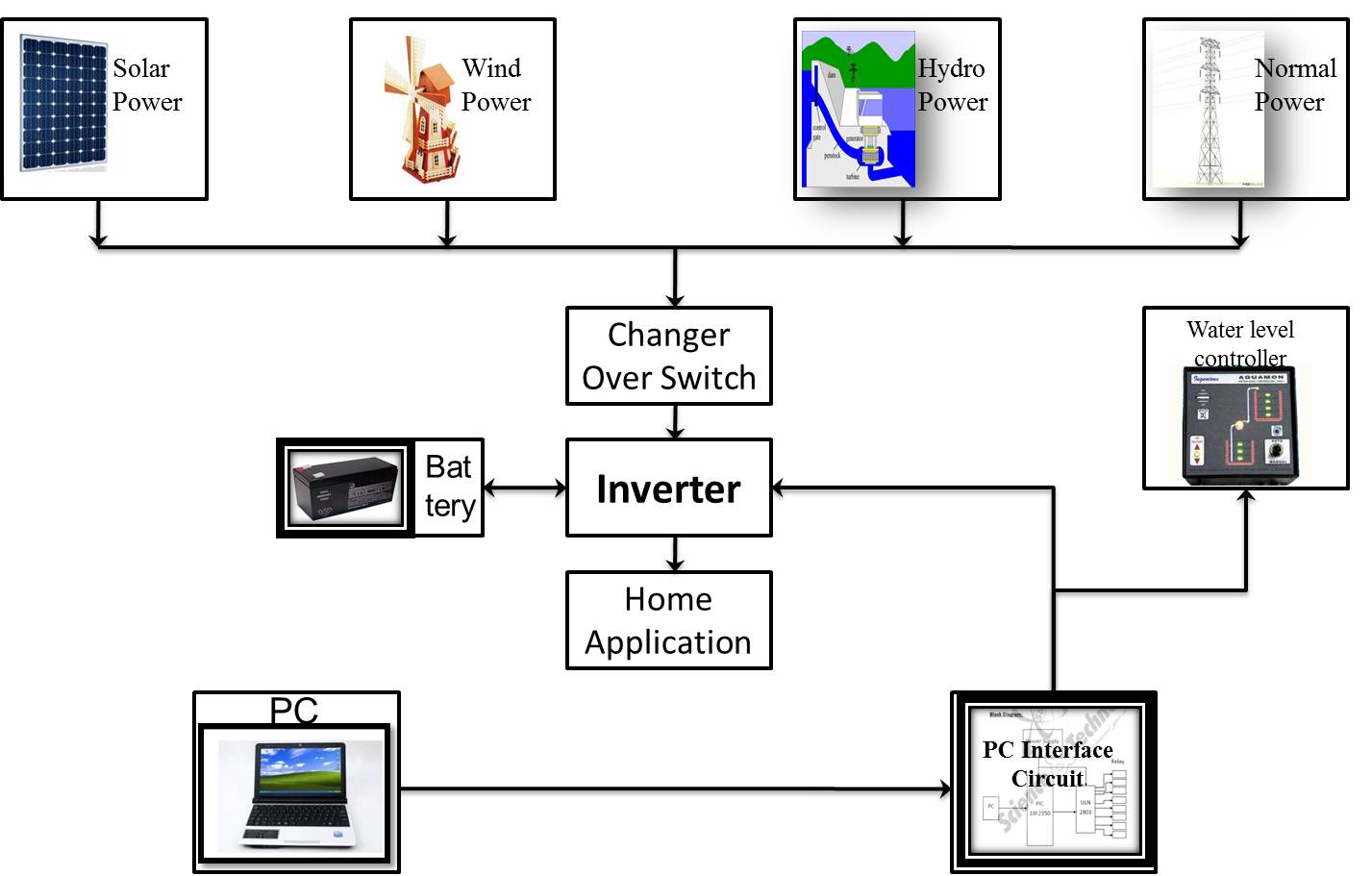
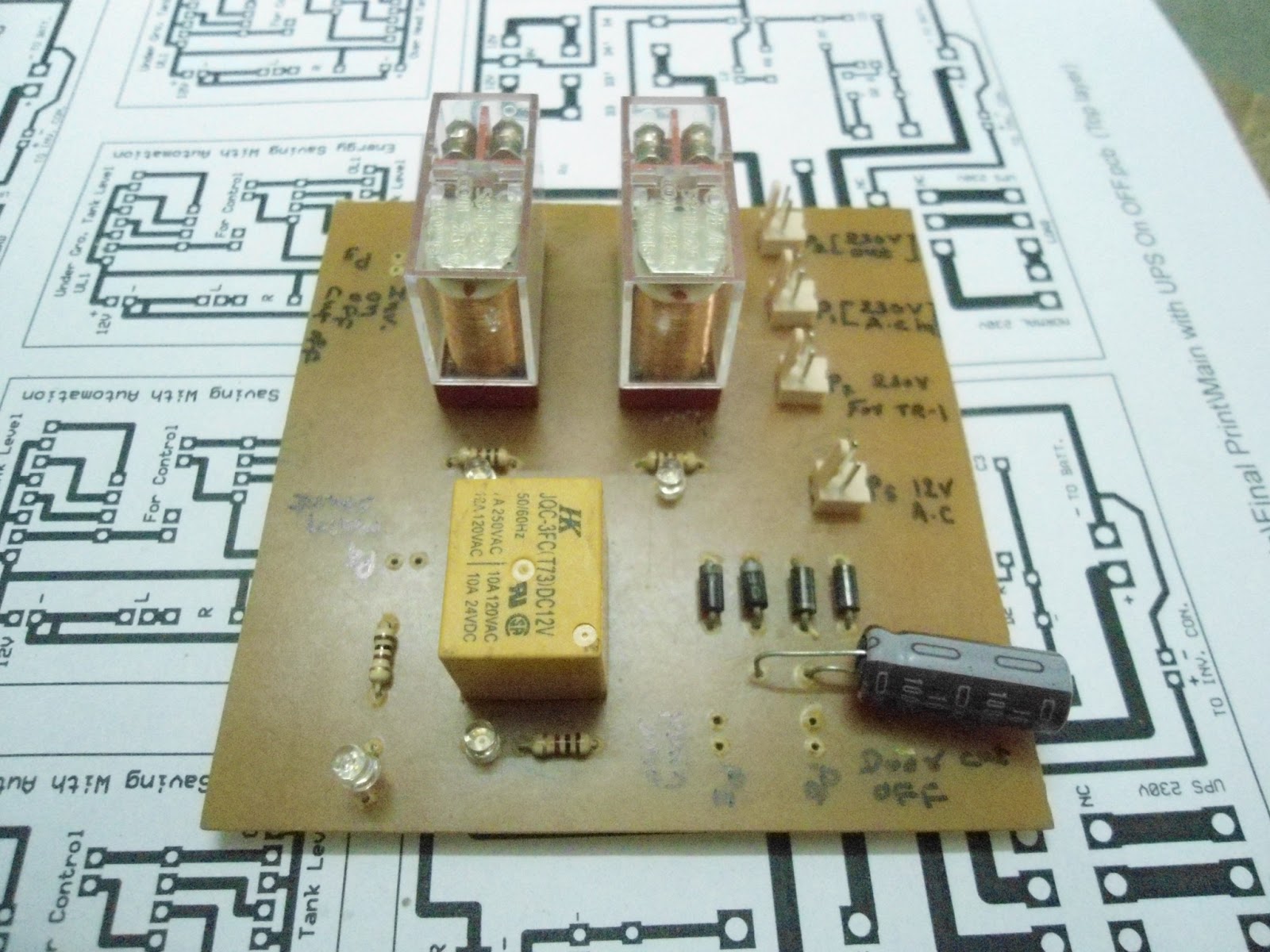
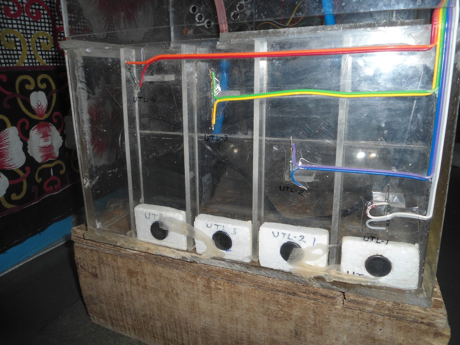
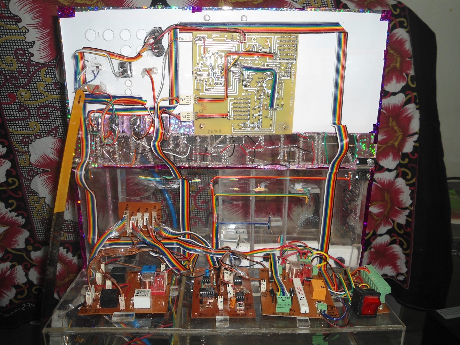
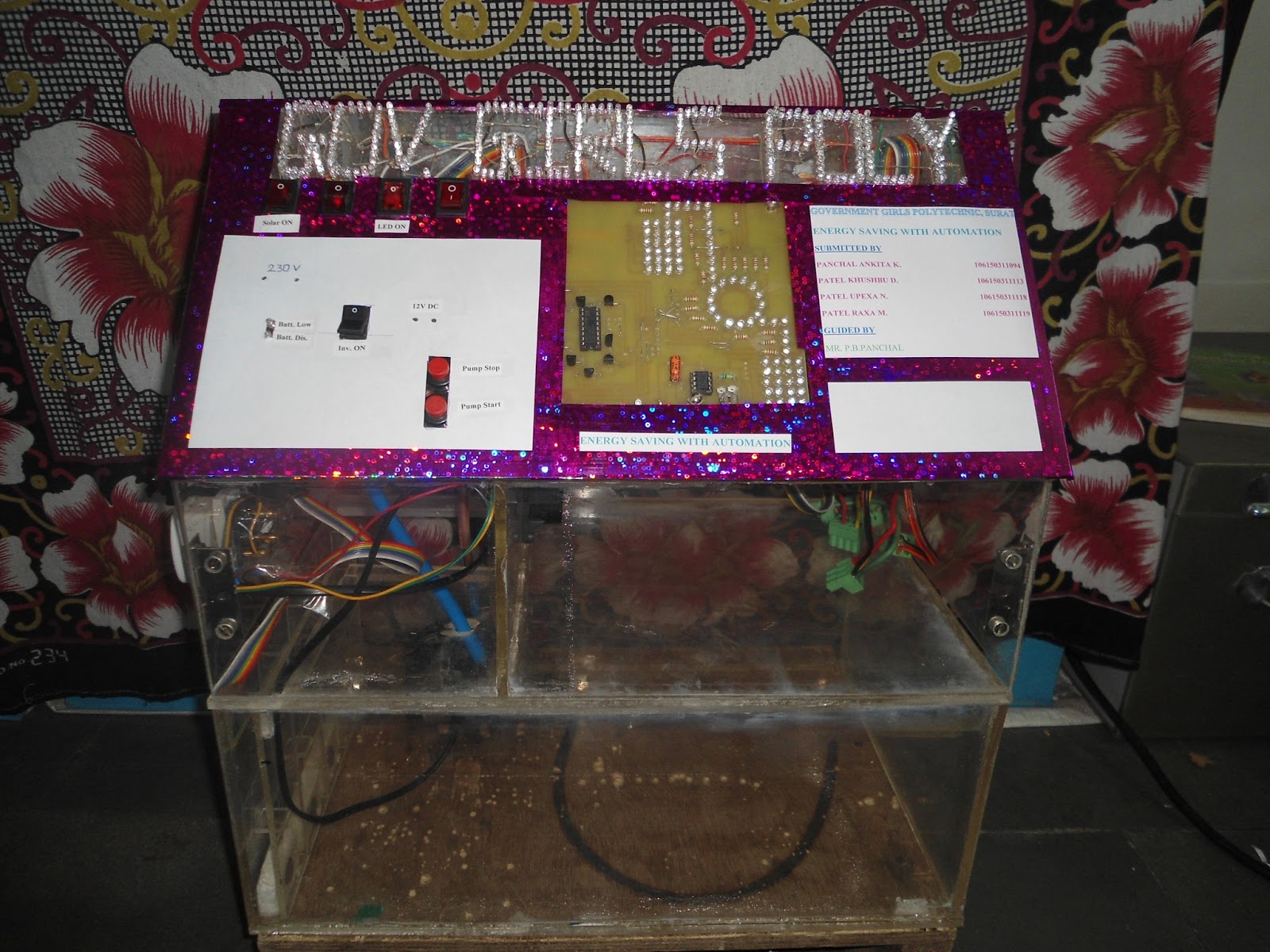
1. Energy Saving With Automation. 2. Solar and wind hybrid system. 3. IC Bread Board. 4. Chaser circuit kit. 5. Electronic ballast. 6. Electronics motor starter. 7. Water level controller. 8. Fully automatic water level controller. 9. 12V, 230V, 200 watt UPS. 10. Water level controller with animation. 11. 3way automatic changer over switch. 12. Chaser circuit kit. 13. Battery charger with voltage level indicator. 14. Automatic dark and light detector. 15 555 Timer. 16 555 LED Flasher.
As mentioned earlier, NMOS (nMOSFET) is a type of MOSFET. A NMOS transistor is made up of n-type source and drain and a p-type substrate. When a voltage is applied to the gate, holes in the body (p-type substrate) are driven away from the gate. This allows forming an n-type channel between the source and the drain and a current is carried by electrons from source to the drain through an induced n-type channel. Logic gates and other digital devices implemented using NMOSs are said to have NMOS logic. There are three modes of operation in a NMOS called the cut-off, triode and saturation. NMOS logic is easy to design and manufacture. But circuits with NMOS logic gates dissipate static power when the circuit is idling, since DC current flows through the logic gate when the output is low.
What is PMOS?
As mentioned earlier, PMOS (pMOSFET) is a type of MOSFET. A PMOS transistor is made up of p-type source and drain and a n-type substrate. When a positive voltage is applied between the source and the gate (negative voltage between gate and source), a p-type channel is formed between the source and the drain with opposite polarities. A current is carried by holes from source to the drain through an induced p-type channel. A high voltage on the gate will cause a PMOS not to conduct, while a low voltage on the gate will cause it to conduct. Logic gates and other digital devices implemented using PMOS are said have PMOS logic. PMOS technology is low cost and has a good noise immunity.
What is the difference between NMOS and PMOS?
NMOS is built with n-type source and drain and a p-type substrate, while PMOS is built with p-type source and drain and a n-type substrate. In a NMOS, carriers are electrons, while in a PMOS, carriers are holes. When a high voltage is applied to the gate, NMOS will conduct, while PMOS will not. Furthermore, when a low voltage is applied in the gate, NMOS will not conduct and PMOS will conduct. NMOS are considered to be faster than PMOS, since the carriers in NMOS, which are electrons, travel twice as fast as holes, which are the carriers in PMOS. But PMOS devices are more immune to noise than NMOS devices. Furthermore, NMOS ICs would be smaller than PMOS ICs (that give the same functionality), since the NMOS can provide one-half of the impedance provided by a PMOS (which has the same geometry and operating conditions).
More Info:- http://www.electronics-tutorials.ws/transistor/tran_6.html


No comments:
Post a Comment